Semiconductor
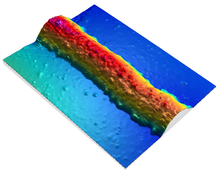
| Stud Bump | 長さ、高さ、体積、粗さ、角度 |
| CMP | Warpage、 粗さ |
| CVD | 粗さ |
| Wafer | Warpage、スクラッチ、粗さ |
PCB
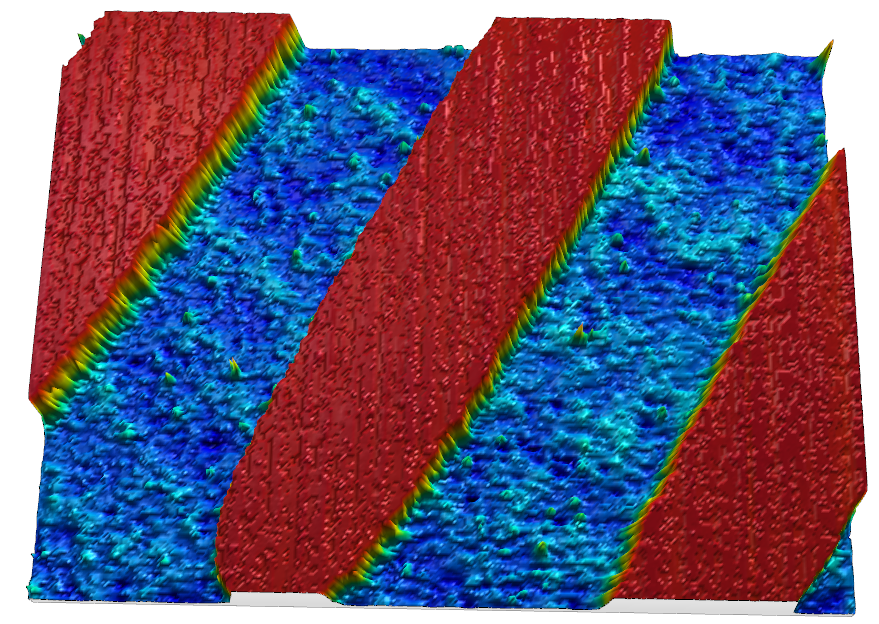
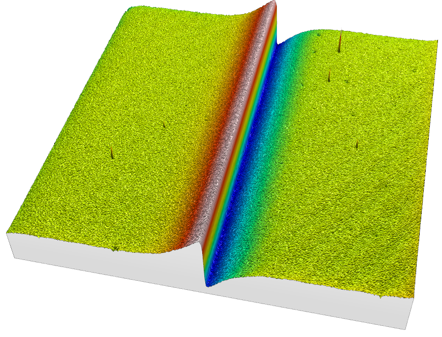
| Substrate (Pad, Trace, Space, Anchor, Land, Ball Pad, Via Hole, Dimple, SR) | 長さ、高さ、幅、深さ、厚さ、粗さ、直径、体積、真円度 |
| BGA | Ball高さ、直径、共平面性 |
Display
| Photo Space | 長さ、高さ、幅、体積 |
| RGB | 厚み、粗さ、BM 厚み |
| TFT Pattern | 高さ、幅、粗さ |
| BLU | 角度、幅、高さ、粗さ |
| Metal Jet | 幅、高さ、角度、粗さ |
| Glass | Defect形態、幅、高さ |
| OLED | 蒸着高さ、角度、体積 |
その他
| MEMS | 高さ、幅 |
| Precision machine part | 粗さ、高さ、幅 |
| Laser Marking | 高さ、体積 |
| Inkjet | 体積、高さ、面積 |
| Micro Lens | 曲率、高さ |
| RFID | 高さ、幅、粗さ |
Specification
| Vertical Resolution | VSI,VEI < 0.5nm, VPI < 0.1nm |
| Lateral Resolution | 0.05~7.2um(Depends on magnification) |
| Height Repeatability | ≤0.1% @ 1σ |
| Objective Lens | 5 Selectable(Automatic) |
| Zoom Lens | 3 Selectable(0.55x/0.75x/1.0x @ Automatic) |
| Camera Format | 1/2″ Mono Camera |
| Scan Method | Piezo Actuator@Capacity Closed loop |
| PZT Scan Range | ≤150um |
| Scan Speed | 7.5um/sec(1x) / 22.5um/sec(3x) |
| Illumination | White LED |
| Filter | Visible/Bandpass/Green Filter(Auto) |
| Auto Focus | Yes |
| X/Y Axis Stroke | 300mm(X) x 300mm(Y) |
| Z Aixs Stroke | 100mm |
| Tilt Aixs Stroke | ± 5° |
| Work Table Size | 350mm X 350mm |
| Max Workpiece Load | ≤ 10kg |
| Layout Size | 1780mm(W) x 960mm(D) x 1500mm(H) |
| Software | Surface View/Surface MAP@ Window10 (64bit) |
| Stitching | Yes |
| Vibration Isolation Platform | Passive Type(Vertical Resonance: 1.5Hz) |
| Input Power | 2∮,110V/220V(±10%), 50/60Hz |
Option
| Interference Lens | 2.5x, 5.0x, 10x, 20x, 50x, 100x |
| Objective Lens | 2.5x, 5.0x, 10x, 20x, 50x, 100x |
| Zoom Lens | 0.55x, 0.75x, 1.0x, 1.5x, 2.0x |
| PZT Scan Range | ≤300um |
| Motor Scan | ≤10mm@Linear Scale |
| Laser Auto Focus | Option |
| Camera Format | 2/3″ or 1″ Mono Camera |
| Work Table | Vacuum Table, Rotation Table |